A step-by-step guide on working with PCB data in Simcenter 3D
This post is the second part of three about creating an electronics systems cooling (ESC) digital twin to meet thermal requirements. Read part one here.
Simcenter 3D provides advanced geometry preparation, meshing, and mesh editing tools that enable efficient and robust management of the ESC digital twin.
Step 1: Import the PCB data into Simcenter using the PCB Exchange application.
The ECAD data is provided in IDX format, which is read in and interpreted in the PCB Exchange application (other formats, such as ODB++, are also available).
Two options for importing the data:
- Import the entire geometry including all the mounting holes and vias
- Filter out small features
In the video below, we choose to filter out small holes and pin holes. Vias will be modeled downstream using the conductivity map.
PCB Exchange creates the necessary geometry for each component and the board, and also creates an assembly and positions the components on the board.
- The copper traces in the PCB are modeled using a conductivity map generated from the ECAD data available in the IDX file.
- The vias may be imported now or selectively imported and modified using the advanced conductivity options.
- The board conductivity is computed, and the field is saved to an xml file that can be previewed in the web explorer tab. To improve the resolution of the computed field, simply increase the number of calculation points.
- In this example, the number of calculation points is increased from 100 to 300. The resulting conductivity field is more detailed and captures smaller features on the PCB.
Step 2: import the PCB into the electronics package.
Given that Simcenter sits on top of NX, a number of powerful tools are available to easily import the PCB.
Assembly Constraints
- Fix the bottom cover using Assembly Constraints. This is good practice because is provides a reference against which all other Assembly Constraints are computed.
- Apply Assembly Constraints to place the PCB into the correct location. In this case, the center lines of two bolt holes are aligned and the bottom of the PCB is in contact with the mounts.
- With the PCB correctly positioned, any changes to the underlying geometry will be correctly propagated upstream.
Immersed Boundary Method
IBM solves the challenges of performing fluid flow simulation for complex geometries. In particular, it significantly simplifies the extraction of the fluid domain and the subsequent meshing.
With IBM, the cavity inside the part is detected and meshed automatically. The resulting mesh does not conform to the walls, and the solids themselves are immersed in the fluid mesh. The solver resolves the walls, and boundary conditions can be applied on geometry, maintaining full associativity with the design geometry.
All of this results in a faster workflow for fluid mesh generation and model preparation. For example, the headlamp geometry shown here was meshed in approximately 40 seconds.
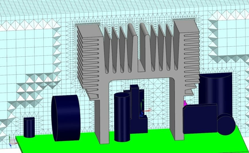
In this example, a box that represents the air domain has been created ahead of time.
- Using the Point Selection tool in Simcenter, choose a point inside the domain. Verify that the point is indeed inside the domain, then generate the air mesh. The process takes only a few seconds.
- Because the resolution selected is larger than the slot sizes, the mesh does not include the region inside the package. To change this, turn on Automatic Refinement. This will detect smaller features up to the specified refinement level and apply local mesh size reductions. Remeshing takes only a few seconds. The mesh now covers the entire air domain and captures the internal geometry correctly as well.
For IBM, the solid components must be meshed with 3D or 2D elements, and the boundary conditions must be defined on null shells.
- Start by creating 2D shells on the inlet faces.
- Modify the mesh collector to use the properties of a null shell. Turn off the radiation properties, as these shells are only used by the fluid boundary conditions.
- Define the openings in the same way.
PCB Exchange automatically creates shell meshes on top of the board and the components. To use the immersed mesh solver, the remaining unmeshed faces must be meshed with 2D shells. The board bottom mesh is dependent on the top mesh.
Step 3: include the relevant physics for the simulation.
How can you efficiently create the thermal/flow model of an electronics package, given the need to account for multiple loads, dissipations, and thermal couplings? The workflow from PCB Exchange to Simcenter 3D Electronics Systems Cooling delivers significant savings both in time and labor.
In PCB Exchange, use Create ESC to create the thermal/flow simulation
- Define the correct file paths, and point to the component thermal database. This xml file contains thermal characteristic data, including dissipation, resistance values for resistor models, as well as the maximum allowed temperature.
- Explore and edit the component catalogue through its dialog.
- Point to the previously calculated board thermal conductivity file. As PCB Exchange automatically creates a complete ESC solution, this thermal analysis is ready to run. It also creates expressions for the thermal loads on the components, which will help when setting up optimization runs.
- Import the simulation objects and solution into the electronics package sim file, which contains a thermal/flow solution with the PCB-related simulation objects in a dedicated folder.
- The solver generates a report of all the component temperatures and highlights those that have exceeded the threshold temperature. The temperatures of specific components may also be tracked during the solve.
Step 4: Create the flow boundary conditions and the thermal couplings
Create thermal couplings in two ways. The automatic face detection in the Surface-to-Surface Contacts simulation object helps to speed up and simplify the workflow, organizing the resulting Face-to-Face Contacts in the Thermal Couplings folder. Any remaining couplings can be created and added manually.
This example demonstrates how to create the thermal coupling between the board and the bottom case.
We will use Selection Recipes to define the inlet flow boundary condition to account for any potential geometry changes. In addition, we will specify the boundary condition using an expression to prepare for optimization later.
- Use a selection recipe to pick out the inlet faces.
- Create an expression for the inlet flow rate, one of the optimization variables.
- Use the Inlet faces Selection Recipe and the Inlet flow rate expression in creating the inlet boundary.
- Create the openings on the faces with null shells. In this example, we are assuming that the electronics package is effectively contained in a mostly enclosed space.
- Keep things organized by placing the flow boundary conditions into their own folder.
Step 5: inspect the thermal response to the imposed loads and boundary conditions.
Simcenter 3D offers powerful post processing tools and a number of informative and instructive ways to visualize the results.
- Layout views in Post allow you to recreate the desired layout of results with one activation. In this example, the board temperatures are displayed immediately.
- Two other Layout States show the slot configuration for the top and bottom covers. The Layout States will be used for the post processing of the optimization study in the design space exploration and optimization software HEEDS.
- Visualization tools are also effective in design exploration, as we will see in our next post. With the baseline simulation completed, we are ready to setup the optimization study and find the optimal design.
Read the third and final post of this series to learn how to set up an optimization study in Simcenter 3D to find the optimal design.
Learn more about Simcenter 3D